PROJECT 04
High-Performance RISC-V Processor with 3-Stage Pipeline on FPGA
Custom Verilog implementation with fetch, decode/execute and memory/writeback stages, verified on Xilinx Nexys A7.
3
Pipeline stages
6
RTL cells
245
Nets in design
RISC-V
Custom ISA
Overview
A custom RISC-V processor implemented in Verilog, refactored from a single-cycle baseline into a 3-stage pipelined microarchitecture to raise instruction throughput. The design was elaborated and verified in Xilinx Vivado and deployed on a Nexys A7 development board.
The work covers the full RTL stack: fetch, decode/execute and memory/writeback pipeline stages, the register file, ALU and control unit, plus the pipeline registers and forwarding logic needed to make the pipelined datapath behave correctly.
The engineering motivation is throughput without changing time-to-completion for any single instruction: by decomposing the single-cycle datapath into pipelined stages separated by registers, multiple instructions occupy different hardware resources in the same clock cycle, allowing the design to run at a higher operating frequency and raise overall IPC on non-dependent instruction streams.
System Architecture
Fetch (IF)
PC → instruction memory → IR; PC + 4 update path
IF / ID Pipeline Register
Latches PC and IR at stage boundary
Decode & Execute (ID/EX)
Register file read · immediate gen · ALU · branch condition
EX / MEM Pipeline Register
Latches ALU result and control lines
Memory & Writeback (MEM/WB)
Data-memory load/store · writeback mux into register file
Hardware
| Subsystem | Selection & Role |
|---|---|
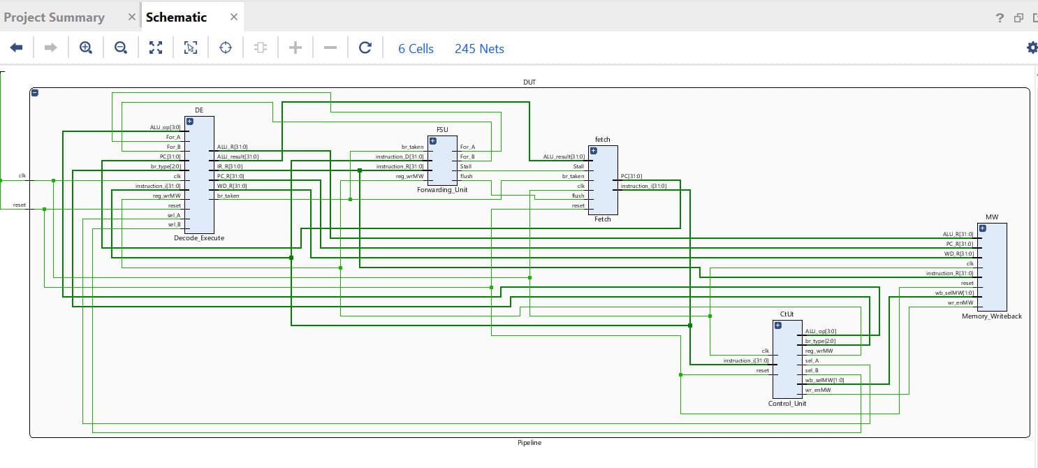
| Fetch stage | Program counter, instruction memory interface, PC + 4 increment path, branch-taken handling |
| Decode / Execute | Register file (read ports), immediate generator, ALU (all supported RV opcodes), branch-condition unit, forwarding sources |
| Memory / Writeback | Data-memory interface for loads and stores, writeback mux selecting between ALU result and loaded data into the register file |
| Pipeline registers | PC and IR latches (IF↔ID), ALU-result and control latches (EX↔MEM), driven by the same clock with synchronous reset |
| Control unit | Decodes instruction fields into ALU op, register-write enable, source-operand selects, writeback-select, memory-write enable and branch type |
| Forwarding unit | Resolves EX-stage data hazards by selecting forwarded operands from later pipeline stages when register dependencies are detected |
Key Engineering Work
- RTL refactor of a single-cycle CPU into a 3-stage pipelined datapath with correctly sized pipeline registers at each stage boundary
- Full-CPU integration in Verilog — instruction memory, register file, immediate generator, ALU, branch unit, data memory and writeback path — assembled under a single configurable top-level
- Forwarding logic to resolve EX-stage data hazards without stalls on the common case, verified against dependent instruction streams
- Vivado-based synthesis, elaboration and implementation flow targeting the Xilinx Nexys A7 FPGA, with elaborated schematic review used as a design-intent check
- Verilog testbenches with waveform-driven debug for cycle-accurate verification and root-causing pipeline hazard behaviour
Results & Validation
Pipelined design successfully elaborated in Vivado as a hierarchical top-level containing Fetch, Decode_Execute, Forwarding_Unit, Memory_Writeback and Control_Unit modules (6 cells / 245 nets in the elaborated schematic).
Cycle-accurate execution of a hazard-free assembly program verified in simulation, confirming correct pipeline register behaviour across stage boundaries.
Configurable RTL (pipelined vs non-pipelined via a synthesis-time define) preserved as a bring-up and regression aid.
Design successfully targeted the Xilinx Nexys A7 platform via the Vivado toolchain.
Technical Stack
RTL & ISA
- Verilog / SystemVerilog
- Custom RISC-V core
- 3-stage pipelined datapath
- Pipeline registers
- Forwarding unit
- ALU, register file, control unit
FPGA Toolchain
- Xilinx Vivado
- Elaborated schematic review
- Synthesis + implementation
- Waveform simulation
- Configurable top-level defines
Target Platform
- Xilinx Nexys A7 (7-series)
- On-board clocks and I/O
- Instruction / data memory modelled in RTL
- Bring-up and regression testbenches